
| Search our quarter-million Q&As |
Home of the finishing HOTLINE since 1989
-----Achieve uniform thickness in electroplating
Q. I am trying to produce electro-permanent magnets using electrodeposition of sequential layers of copper, iron, and cobalt-platinum(CoPt) on a steel substrate. I attached simplified pictures of the setup. The z-axis (gold color) moves in and out of the bath holding the substrate and allowing it to mate with the mask while the mask is clamped to the bottom of the bath. The anode (grey) is simply submerged in the bath.
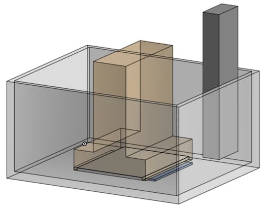
Lastly, I also attached a picture of the mask(blue) with a sample pattern where my goal is to plate in between the red extrusions.

However, before I build this, I would love to ask some questions to prevent potential pitfalls.
Questions:
1. How do I ensure uniform plating across all the cavities in the mask (i.e., use of brighteners, thieves, shields, auxiliary anodes, etc.)?
a. I know that many brighteners are proprietary, but I was thinking of starting with Saccharin and seeing where this gets me. What would be some other simple brighteners that I could use?
b. Could the z-axis serve as a shield (as it covers the top surface of the substrate exposing only the bottom)? I also experienced a problem before where there would be excessive deposition around the edges of the substrate (cathode), and not much at the actual surface where the mask is. Would making them less sharp help?
2. Any other general suggestions for the setup?
Please let me know if anything needs further clarification.
Thank you!
student/hobbyist - Toronto, Ontario
August 25, 2023
A. Hi John.
Sorry, but I don't understand "while the mask is clamped to the bottom of the bath". Obviously you can't do any plating while the component is sitting against the bottom of the tank, not exposed to the plating solution -- maybe you mean the ram goes down and picks up the adhesive mask? Why not just mask the part first, and you can also mask everything you don't want plated.
However, I think the biggest problem, even before you think about the mechanics of the situation, is how are you going to electrodeposit cobalt-platinum? What is the ratio of cobalt to platinum?
Even the 1372-page "Electrodeposition of Alloys" ⇦[this on
Amazon,
eBay, &
AbeBooks affil links]
doesn't address that alloy. Please consider starting by demonstrating to yourself the ability to plate successive layers of copper, iron, and cobalt-platinum at all before worrying too much about the mechanics of your particular situation.
Luck & Regards,

Ted Mooney, P.E. RET
Striving to live Aloha
finishing.com - Pine Beach, New Jersey
Need quick confidential answers? $25
Need project assistance? $100/hr.
Q. Thanks for the reply Ted!
In terms of cobalt platinum, I have seen different papers on this topic with the composition of the bath needed for plating. For example: Dinitrodiammine-platinum 0.05 M, Cobalt Sulfamate 0.0515M, ammonium citrate 0.1M from
https://transducer-research-foundation.org/technical_digests/HiltonHead_2018/hh2018_0136.pdf
I was successfully able to plate layers of iron and copper (did not do platinum yet since it requires quite a bit of money to purchase the chemicals), and now I am looking for a way to do through mask deposition. The ram goes down, and as it moves, the cathode (which is attached to the ram) mates with the mask (which is sitting at the bottom of the container). There is still electrolyte flow in the holes between the mask and the cathode which I expect to deposit on the cathode. On the picture of the mask that I attached, think of the blue surface as the bottom of the container, and red extrusions as the mask. The plating should occur where there is just free space for the electrolyte to flow(between the mask extrusions).
Please let me know if I can provide more details.
- Toronto, Ontario
September 10, 2023
|
|
A. If I am understanding this correctly that the surfaces to be plated are facing DOWNWARD - this will NEVER work at all as described. Period. Full stop. - Czestochowa, Poland A. John, if I understand correctly you wish to use a series of masks which are placed at the bottom of a small home sized electroplating vessel to layer various alloys in sequence. - Ballarat, Australia February 15, 2024 |
Multiple threads merged: please forgive chronology errors and repetition 🙂
QUICKSTART:
We don't want to lose new readers to technospeak, but we also don't want to talk down to folks who may well know a lot more than us :-)
Thus this sidebar -- intended not for the original posters, but for any readers interested in the subject but having some difficulty following it :-)
When electroplating things, they are immersed in an aqueous (water-based) solution, and a source of direct current is attached; in the industry we often call that power supply device a 'rectifier'. The piece you are plating onto is negatively charged (made the cathode), and the positively charged electrode is called the anode. Sometimes the anode is designed to dissolve into the solution to be the source of the plated metal. For example, if you are plating something with nickel, the anode will be made of solid nickel, or nickel chunks will be placed into a perforated titanium basket.
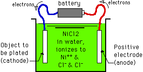
As electricity flows through the external circuit, electrons are pulled from the anode and flow through the external circuit to the cathode. The anode now has a deficit of electrons, meaning that a proportionate amount of the anode nickel will be converted from nickel metal (Ni0 atoms) to Ni++ ions. The nickel anode metal is thus dissolving into the solution as positively charged nickel ions.
Meanwhile, the cathode is accumulating a surfeit of electrons, and this is attracting those positively charged nickel ions to it. When they reach it, the electrons neutralize the positive charge on the Ni++ ions, and they become nickel metal (Ni0 atoms) once again. It takes two electrons to reduce one Ni++ ion to an atom of nickel metal (Ni0). Thus there is a direct correspondence between how much electricity flows and how much metal is deposited. In fact, Faraday's Law says essentially that 96,485 ampere-seconds will deposit one gram equivalent weight of the metal. An ampere-second is one ampere flowing for one second; if the product of the amperes and seconds is 96,485, that deposits one gram equivalent weight of metal.
But imagine that the current is off, and you instantaneously go to full throttle. The electrons move at the speed of light from the anode to the cathode, but the dissolution of the anode and migration of the ions though the solution happens much slower. So what happens at the cathode when there is a huge excess of electrons accumulating, and insufficient nickel ions to satisfy them? They start pulling hydrogen (H+) out of the water, leaving hydroxide (OH -) behind. As the H+ meets the electrons, the hydrogen bubbles out of the solution as hydrogen gas. So Faraday's Law actually tells us that 96,485 causes one gram equivalent weight of something to be reduced, but it might actually work out as 90% of a gram equivalent weight of nickel and 10% of a gram equivalent weight of hydrogen. This would be called 90% efficiency. Too much current density will cause too much of this inefficiency and other difficulties which result in a roughness and poor plating defect called 'burning'.
Ignoring this 'efficiency' stuff for a bit, we see that the amount of plating is directly proportional to the amount of current. Thus, if a component has some spots which are close to anodes or for some other reason draw more current than other areas, the plating will be thicker there. This thread is basically about what can be done about that situation ...
The easiest fix, but only partially effective, is organic addition agents (brighteners) added to the solution which are also drawn to those high current density areas and get in the way of metal deposition, thus assisting in making it more uniform.
Other things that can be done besides ideally locating the anodes with respect to the parts include:
1. Thieves -- These are metal pieces connected to the cathode, designed to draw electricity themselves, and placed very near the high current density area of the part so they steal some of the electricity and prevent the actual part from 'burning'. Thieves represent deliberate waste and are rarely used except in chrome plating.
2. Shields -- These are pieces of non-conductive plastic of any size or shape, usually made of PVC or polypropylene, which are placed in specific spots in between the anode and cathode to block the 'shortest path' to minimize burning and achieve a more uniform current and thickness distribution.
3. Auxiliary Anodes -- These are metal pieces, sometimes made of plating material, but more often made of non-dissolving metals, which are connected to the anode and placed in specific places near the cathode. For example, if you wish to fully plate a wheel or a truck bumper which has deeply recessed areas, you might put an auxiliary anode near that area to reduce the anode-cathode distance so more current will flow to that area.
Q. Hi,
Electroplating usually coats a non-uniform thickness film. I would like to know how this can be overcome such as in high precision electroplating. Thanks in advance.
Regards,
Robin Francois- Boston, Massachusetts
1999
A. Hi Robin. Yours is a pretty broad question I'm afraid! Actually, electroplating CAN deposit fairly uniformly on very simple partsand, barring other factors, Faraday's Law dictates that it will (at 100 percent efficiency, 96,485 amp-seconds will always deposit one gram equivalent weight)
So if the current distribution is uniform, the plating thickness will be uniform. But to even out the thickness when geometry favors higher or lower current density to certain areas, three "mechanical" techniques are shielding (the use of plastic shields to block off the shortest path), thieving (the use of conductive wires as cathodes to steal some of the current away from high current areas, and auxiliary anodes (anode material in close proximity to the work in the areas which need more current).
One or more of these should fix your problem. Good luck.

Ted Mooney, P.E.
Striving to live Aloha
finishing.com - Pine Beach, New Jersey
Need quick confidential answers? $25
Need project assistance? $100/hr.
Q. What are the wetting and leveling agents that are used in Microfabrication?
In MEMS fabrication, I have heard that they use wetting agents and leveling agents in order to be able to electroplate in very small areas such as deep holes for example. What are those agents? Are there other agents or other ways that can be used to do that? And what is the effect of those agents on the plating process?
Robin Francois [returning]- Boston, Massachusetts
2005
A. Hello again Robin.
"Brighteners" are organic addition agents that are drawn to high current density areas and, by being there, tend to somewhat shield those areas from plating, thus driving the plating towards occurring elsewhere. They are often used in plating of all types to force more adatoms for a denser, harder, brighter, less porous plate. To an extent they may also contribute to more uniform plating thickness. In the case of MEMS and thru-hole plating in circuit boards, the brighteners are such large molecules that they cannot easily fit into the holes; thus they shield everything but the holes they can't fit into, and that promotes the leveling. These agents are proprietary; the suppliers who have spent small fortunes developing them and will not tell you what they are; rather, they will simply sell you the copper plating bath or brightener so you effectively license their technology "by the gallon".
For your MEMS issues, L.T. Romankiw's "A path: electroplating through lithographic masks in electronics to LIGA in MEMS" published in Electrochimica Acta, Vol 42, Nos 20-22, pp. 2985---- by Elsevier Science is invaluable. I have what looks to be a reprint from Pergamon Press labeled as "PII: S0013-4686(97)00146-1" (whatever that means). You'll find it behind all the familiar paywalls.
For now at least, you can view for free a very similar presentation by Romankiw titled "Electroforming of Electronic Devices"
Good luck.
Ted Mooney, P.E.
Striving to live Aloha
finishing.com - Pine Beach, New Jersey
Need quick confidential answers? $25
Need project assistance? $100/hr.
A. If the object to be plated is not mechanically complex, you can try plating using anodes of the same shape in close proximity. Thieving, additional anodes, and shielding are otherwise essential for complex shapes.
Jeff Verive- Bolingbrook, Illinois
A. Hi Robin. All plating is not necessarily Electroplating. You can achieve very even finishes all over parts by using autocatalytic plating (ELECTROLESS Plating). There are Electroless solutions available that will provide answers to most finishing situations, but the cost is not cheap.
Regards

John Tenison - Woods
- Victoria Australia
Q. Dear Sir,
Can you suggest some automation methods to form uniform coating thickness .
We carry out copper plating in very conventional manner and the deviation of the coating thickness varies a lot, up to 100-200 microns sometimes.
Is the any sort of automation process that can help to control the variation in microns?
Or should I find a rectifier of higher pulsing rate or anything else?
Please help.
Engineer - Mumbai, Maharashtra, India
November 27, 2012
A. Hi Jack. We appended your question to an existing thread which may go a long way towards answering it. Properly designed plastic shields may be the easiest resolution, but send us a pic or sketch of the parts and the racking and we may be able to refine the answer.
In the electroforming of stampers for CDs/DVDs, the stamper is mounted on an axle and rotates during plating, which can help uniformity. Good luck.
Regards,
Ted Mooney, P.E.
Striving to live Aloha
finishing.com - Pine Beach, New Jersey
Need quick confidential answers? $25
Need project assistance? $100/hr.
Q. I have recently developed a plating rack that holds 198 lug nuts/Wheel locks. I modified the post length (current rack has all the same post lengths) to change the distance between the anode and the work. The result is almost completely uniform plating within 0.1 mils for nickel. The rack looks similar to a lens or a 3-D diamond shape now. We reduced the variation in thickness from around 16-20% across the rack to less than 2%. That 2% is coming from the 8 corner pieces now. Without using conductive thieves (wasting nickel) how can we stop the build up in the corners? Any ideas? I can send a CAD drawing of the current rack and the new "modified rack" to an email.
I really appreciate any help!!
Sincerely,
- Buffalo, New York, USA
December 26, 2012
A. Hi Thomas. Graphics emailed to [email protected] for posting here are always welcome.
Shields are the easy way. These are simply small PVC or polypropylene strips through which current cannot pass, but must go around. They thereby increase the anode to cathode distance to whichever lug nuts they are shielding. They do not need to be solid sheets either: they can be perforated to only partially block the path from anode to cathode, thereby reducing the current to that area without stopping it.
Unless you want to invest in electrochemical modeling software, though, it will take a lot of tinkering and trial-and-error to get the exact results you seek. But you seem to already be quite accomplished at that tinkering :-)
Regards,
Ted Mooney, P.E.
Striving to live Aloha
finishing.com - Pine Beach, New Jersey
Need quick confidential answers? $25
Need project assistance? $100/hr.
Improving throwing power on nickel baths
Q. Hello all.
I need to improve the nickel throwing power in parts that we currently plate for a customer in US.
Those parts are ABS, so they enter copper bath first, having good covering on very recessed area. The problem is that when they go into the semi bright, then bright nickel this recessed area is not 100% covered, getting a defect we call "exposed copper".
I have tried painting this area using a chrome spray paint, but our customer does not accept it.
Some plating conditions:
- semi bright: 11 minutes, 4 amp/dm, ph:3.8, 60 °C
- bright nickel: 11 minutes, 4.5 amp/dm, ph:4, 60 °C.
Thank you in advance for the help.
Bernardo
process engineer - Guadalajara, Jalisco, Mexico
May 29, 2014
A. Hi Bernardo. I doubt that you will fully achieve the results you need by a chemical adjustment to your nickel plating baths alone. But I think you should look into auxiliary anodes as the most promising solution, and I'm quite confident they will solve the problem. Best of luck.
Regards,
Ted Mooney, P.E.
Striving to live Aloha
finishing.com - Pine Beach, New Jersey
Need quick confidential answers? $25
Need project assistance? $100/hr.
|
A. Hello Bernardo, Process Engineer - Malone, New York USA A. Bernardo, - Kitchener, Ontario, Canada |
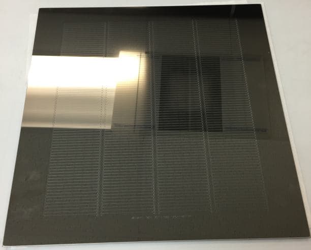
Q. I'm having a problem getting uniformity in electroplating Nickel-cobalt on a 12 X 12 square glass substrate with a photo resist mask. (33 gal tank with sparger at the bottom running through the center of the anode and cathode). No matter what I do I get Bottom heavy. I've moved the sparger toward the anode; it caused my plating to be slower but still bottom heavy. When I moved it toward the cathode it plated faster but still bottom heavy. Same thing when I had the sparger straight vertical always bottom heavy. I've tried shielding, flipping it, plating very slow -- still same results. Do you think it's how far the sparger is replenishing solution at the bottom causing the bottom to plate quicker? Have so many question no one to give me answers.
hero chea- lowell, Massachusetts
December 1, 2014
A. Hi hero. No, I don't think so. Although everything matters to some extent, I don't think the position of the sparger is the main driver. The main problem is that the current density on the bottom of the rack is too high. For one thing, your anodes need to be shorter than the length of the rack, i.e., the lowest point of the work in the tank must be lower than the lowest point on the anodes. For another thing, it is always possible to build shields which will prevent heavy buildup. Good luck.
Regards,
Ted Mooney, P.E.
Striving to live Aloha
finishing.com - Pine Beach, New Jersey
Need quick confidential answers? $25
Need project assistance? $100/hr.
A. Hi Hero
12x12 what? mm, feet yards? And a glass substrate is not noted for its conductivity!
However to address your problem try this.
Put an anode horizontally on the bottom of the tank and smaller than the workpiece. (insulate the lead or that will act as a side anode)
Turn the sparger off and suspend the work piece horizontally above the anode and FACE UP away from the anode. It will need to be some way below the bath surface to allow a reasonable current path. It may still be worth using some shielding for the edges but it should help.

Geoff Smith
Hampshire, England
A. I agree with Ted. What many people do not consider is some of the + charged ions go in all directions from the anode. Some reflect off of the bottom of the tank, thus heavier plate on the bottom of the part.
Shields and robbers work but it is simpler to just raise the anode up if you do not have shorter anodes.
I have heard of people taping off the bottom portion of the anode. I am not in love with this idea, but it is a quick and dirty check of how short you need the final anode.
- Navarre, Florida
Q. Should I build a shield for the work piece or a shield for the anode? If these pictures of my setup will help...
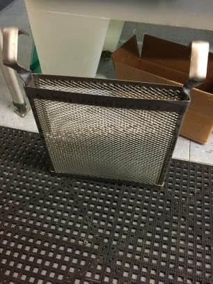
That's the tank, work piece and anode basket ⇦ huh? but the basket I'm using right now is smaller then that one.
hero chea [returning]- lowell, Massachusetts
December 15, 2014

A. Hello again Hero. Are you bringing the power into your rack via an alligator clip to a small diameter titanium screw? Not very reliable.
I can't totally figure out your racking (and shielding, if any). And I guess I'm seeing that your part is glass and we can see through it, but I'm not sure. This brings up the point that Geoff implied, regarding how is the glass metallized so you can electroplate it.
But the point that James and I were making is that it looks like your anode basket may be too deep. It should end 2 or 3" further from the bottom of the tank than your plated part ends. If the only problem is a bottom-heavy deposit, try that. For a quick trial, just wrap plater's tape ⇨
completely around the several bottom inches of the basket as a shield, so that no current can flow from the bottom several inches. Good luck.
Regards,
Ted Mooney, P.E.
Striving to live Aloha
finishing.com - Pine Beach, New Jersey
Need quick confidential answers? $25
Need project assistance? $100/hr.
A. Hello Hero,
I had to make adjustments to Acid Cu anode baskets in the PC board industry. We were getting 15% higher thickness variation on the bottom of the board. The round Ti anode baskets came 2" below the work. This was an error with the original design / installation of the tanks. Instead of buying 48 shorter anode baskets, we cut 5" lengths of PVDF pipe and slid them onto the outside bottom of the basket. The piping fit snug over the baskets, then we bagged them. We were using 2" high phos cu balls. This solved the thickness variation problem. Because you are using rectangular baskets you could have a plastic fabricator in your area make you rectangular pieces of PDVF to slide onto or fit inside the bottom of the anode baskets. Ted had a good idea of using plater's tape around the bottom of the basket as a test before you take further measures. This anode basket adjustment would save you time in rigging a cathode shield every time you plate your part if a permanent shield on the rack is not possible. Hope this helps!
Process Engineer - Phoenix, Arizona USA
![]() Thanks it worked!! What do you recommend using instead of the alligator clips for power?
Thanks it worked!! What do you recommend using instead of the alligator clips for power?
- Lowell, Massachusetts
A. Hi again. I think alligator clips are okay, but that they should be clipped onto something more substantial so the current doesn't have to travel through that small screw to get to the work.
Regards,
Ted Mooney, P.E.
Striving to live Aloha
finishing.com - Pine Beach, New Jersey
Need quick confidential answers? $25
Need project assistance? $100/hr.
Q. I'm trying to get thickness at ±.00005. Picture of the mandrel is in my last posts. Right now I'm getting .00165 to .00240 throughout the whole mandrel. Any suggestion on how to go about this?
hero chea [returning]- lowell, Massachusetts
December 30, 2014
A. Hello again Hero. Your present variation is ± .000375, and you want to reduce it to .00005 ... that is a huge reduction in tolerance, and I'm not sure whether you can get it even with endless trial & error on shield designs. The first thing I'd do is to plate two substrates as identically as you can, and measure the thicknesses on both the same way to be certain that any thickness variation is reliably tracking the "geography" of the substrate, and is not being influenced by factors that are still "random".
If you are at the point, or can get to the point, where there is essentially no thickness variation other than that which is clearly mappable to the location on the substrate, then you can start blocking the current to the HCD areas with shields.
It wouldn't be easy, but you could mount the plate on an axle and rotate as it's plating, this is done for stampers for CDs. Good luck.
Regards,
Ted Mooney, P.E.
Striving to live Aloha
finishing.com - Pine Beach, New Jersey
Need quick confidential answers? $25
Need project assistance? $100/hr.
|
A. You might want to try increasing air agitation ⇦ huh? and using a lower amperage, but not so low as it becomes a solution dummying operation. James Watts- Navarre, Florida A. Hi again Hero Geoff Smith Hampshire, England |
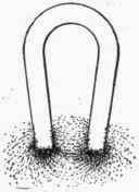
![]() Thanks Geoff. Okay, 'reflecting' was not the precise word, but it might help people recognize & visualize that the current flow & ion movement is not restricted to the shortest path, but includes bulged out paths from anode to cathode that will reach the bottom of the tank. Maybe the magnetic lines of flux around a horseshoe magnet are a good visual of the ionic current flow from anode to cathode?
Thanks Geoff. Okay, 'reflecting' was not the precise word, but it might help people recognize & visualize that the current flow & ion movement is not restricted to the shortest path, but includes bulged out paths from anode to cathode that will reach the bottom of the tank. Maybe the magnetic lines of flux around a horseshoe magnet are a good visual of the ionic current flow from anode to cathode?
I discovered the implications of this when I assumed that 18 volt rectifiers would be plenty big for a particular nickel plating installation because they were 50% higher voltage than hundreds & hundreds of successful installations before it :-)
... but in this particular case we were plating large steel sheets at a steel plant and the anode-to-cathode distance was large AND there was essentially no bulged out paths, and "gut feel" betrayed us. In this case although the solution resistivity was where it was supposed to be, the solution resistance was very much higher than we expected because there are no bulged out paths when you're plating a huge solid sheet.
There are a couple of companies that offer "electrochemical modeling software" that incorporates Finite Element Analysis, and they can probably be found by googling.
Regards,
Ted Mooney, P.E.
Striving to live Aloha
finishing.com - Pine Beach, New Jersey
Need quick confidential answers? $25
Need project assistance? $100/hr.
Q. Hi Ted and others
I am very much interested in shielding, Ted mentioned it as a suggestion to a previous posting of mine concerning issues of high field strength around the edge of a hemispherical bowl (acid copper plating the interior).
I have been struggling a little at the conceptual level regards the mechanism of shielding, I do not for a moment doubt the wisdom of years of practical experience so this is more about my wish to conceptually understand what's actually going on.
Suppose an insulator acted only as a physical (ion) barrier thereby increasing current path length and hence resistance to an area with an intense field, say a point or edge. Then if the insulator does not affect the field only the response of ions to that field then there will still be an area of intense field both sides of the insulator and in particular the region between the sharp point or edge and the shield may become ion depleted and hence cause burning unless we add agitation. However if we add agitation have we not simply undone the whole point of adding a shield - surely we have on one hand increased path length and then on the other hand offered ions a neat short cut by means of bulk import at speeds well in excess of ion migration velocity. Seen from this angle it starts to look a bit self contradictory.
https://en.wikipedia.org/wiki/Electrical_mobility
The key points I am making are that current or ion migration is a response to an electric field, stopping or throttling down ion migration does not imply the field itself is blocked - what happens in the region between the insulator and the sharp edge? this is the area of high field strength, our scenario dictates we have merely partially isolated it - we have not decreased the field strength and so can expect local effects including burning and ion depletion. If we do not encounter some ion depletion then the shield is not working correctly as we have a region between the sharp edge and insulator that still has a high field strength yet we have throttled back ion migration into that area.
Here I think its very important again to distinguish between a field and the current that results from it, in this scenario the insulator is NOT affecting field strength merely the response of ions to that field, we have to think first of field and then of current.
Again - I am not flying in the face of years of practical experience, I am interested in whats actually going on here and we can only do that by asking questions.
Coming from a Physics background I should know all about insulators in electric fields but I must admit I am rusty so I took a quick refresher "course" see this link.
http://physics.info/dielectrics/
The principle of interest here is the way that a dielectric responds to a field between two conductor plates by polarisation, setting up an opposing charge potential that decreases the field strength set up by the charged plates.
Now if the mechanism of the insulator is both to increase path length and so increase path resistance but also to reduce the field strength then there is potentially a double effect here and the reduction of field strength may go some way to answer the issues that I raised above.
To recap if we do not reduce field strength with insulators but merely increase path length then are we not laying ourselves open to a region of now isolated high field strength and so ion depletion which then warrants agitation which undoes the depletion but also arguably undoes the very benefit of increased path length? We seem to have hit a rather circular concept?
If the dielectric polarisation view is to be believed then we have an explanation that breaks the circular argument I suggest above because now the insulator is seen as being responsible not only for an increase in current path length but also as a reducer of high field strengths so we reduce the potential for ion depletion as the core problem of high field strength is reduced - the problem is solved at root cause rather than being side stepped.
If there is sense in this view then it would seem that good shields should be made from plastics with a high dielectric constant like PVC and indeed the same materials used in capacitors would make good candidates for shielding subject to other criteria of course.
It may also be the case that the best shapes for shields might be determined by consideration of symmetry so a rough approximation.
For instance I would guess that the best shape to diminish field strength between two conductors, one a hemisphere and the other a sharp point on the axis of that hemisphere would actually be a smaller hemisphere.
The ideal shape to reduce charge to the rim of a cylinder might be a half bagel ( sliced torus ) kind of shape, of course the shape and positioning of the anode will affect the field so these are only rough approximations, for a more detailed analysis we might consider making a shield shaped like a surface of equi-potential between the cathode and anode surfaces.
Sorry if this seems like a load of navel gazing to some -- it's not for me, I tend to like to proceed into areas like this with a conceptual idea of what's really going on so I hope those who feel differently will not shoot me down with arguments of experience or practicality and see that some folks like to know what's going on under the hood.
- Saltum Denmark
November 18, 2015
A. Hi Jon. You may be viewing it correctly, but I don't think so. I think the ions are not ethereally responding to your 'field strength' argument, but are suffering their way along resistive paths.
As a thought experiment, picture it this way: imagine that ions must travel along copper wires like electrons do. Imagine that you have therefore installed 10,000 small copper wires evenly spaced over the surface of the anode, which then run to the cathode where they are again evenly distributed. Because the wires to the rim area are much shorter and therefore lower in resistance, you get more current flow to the rim, and heavier plating and/or 'burning'.
Put the shields in place and re-hook 10,000 wires. No drilling holes in the shields though, so now the wires to the rim area must go around the shield and are longer than the other wires rather than shorter. Their resistance is higher, so less plating takes place. If you find this thought experiment a stretch, replace the copper wires with small straws full of conductive solution :-)
Although the ions take conductive fluid paths rather than copper paths, those paths have resistance, and I think this is the correct way to picture it, and the way shields actually work.
Regards,
Ted Mooney, P.E. RET
Striving to live Aloha
finishing.com - Pine Beach, New Jersey
Need quick confidential answers? $25
Need project assistance? $100/hr.
|
- Saltum Denmark A. Hi Jon Geoff Smith Hampshire, England |
Luck & Regards,
Ted Mooney, P.E. RET
Striving to live Aloha
finishing.com - Pine Beach, New Jersey
Need quick confidential answers? $25
Need project assistance? $100/hr.
(You're on the 1st page of this topic) Next page >


Sorry! Finishing.com is temporarily Read-Only.
Ted Mooney is retiring but I have several offers to take it over.
We're working hard to make sure we find it the best new home.