
| Search our quarter-million Q&As |
Home of the finishing HOTLINE since 1989
-----Electroforming on to electroforms
2003
Q. I need to know whether it would be possible to perform a second round of electroforming onto electroformed microcomponents -- ie:
1: make components by electroforming, but stop the process before removing unexposed resist
2: plate with mask -- gold? nickel?
3: coat with a second layer of resist
4: expose, develop and electroform
Could this be performed repeatedly? Why not?! Is there perhaps a problem in that the surface of the developed resist + electroformed components is not flat enough?
Many thanks for your answers.
Rupert Griffiths- Cambridge, Cambs, UNITED KINGDOM
A. It's strange that I have been in the plating industry a long time and haven't heard this question because it doesn't sound like it would be an unheard of requirement. I can't give you the benefit of actual experience, but I believe that it should not be a problem if you can maintain good current distribution. Remember that for precision electroforming (stampers, molds, etc.) that it is the first deposited surface (the side closest to the mandrel), not the last deposited surface, that offers the best replicability.

Ted Mooney, P.E.
Striving to live Aloha
finishing.com - Pine Beach, New Jersey
Need quick confidential answers? $25
Need project assistance? $100/hr.
2003
A. Dear Rupert,
What you are describing is possible. As you can imagine the problem is one of registering the second image to the first and also maintaining uniform thickness for the electroformed components across the mandrel.
As an alternative and if the features of your electroform allow, it is possible to electroform the parts so they are thicker than the resist and then lift off the parts. The resist is left on the substrate and a second set of parts can be made from the same patterned area. Lifting off the parts slightly damages the resist edges, so the mandrel does have a finite life.
Good luck with your process.

Pat Mentone
St Paul, Minnesota
2003
A. Multilayer electroforming is possible, but I do not understand what you mean by "stop the process before removing unexposed resist". If you do not develop the image (i.e., dissolve the unexposed resist) you do not have a pattern to electroform. Hewlett Packard have a couple of patents granted in the mid to late 1980's on multilayer electroforming to make ink-jet nozzles. They used positive and negative resists in sequence to get their desired shapes. The problem with using the same resist is that a developer is very similar to a resist stripper, so as you image the second (or later) layers, you start to strip off the initial layers. However, this is easy to overcome, by using different types of resist! Secondly, as you build up the electroform it will become a 3-dimensional shape and that will give problems is getting a good image resolution. Nevertheless, this can also be easily overcome. Thirdly, Pat is right about registering the image; it may be difficult to accurately do so, but there are systems available that can achieve micron scale accuracy if you are prepared to pay for it! Multiple runs with electroforming is not unheard of and relatively high numbers can be achieved by using the correct systems. There is a lot of exciting work being done with LIGA and micro technology at present, so it may be worth looking at these areas. Better still, look at nano-engineering techniques.

Trevor Crichton
R&D practical scientist
Chesham, Bucks, UK
2003
How to get even thickness of deposit in electroforming
Q. Dear Sir,
I want favor from you of how to control uniform thickness in electroforming process. Now in process I am unable to produce uniform thickness of shim/mandrel. Due to this I am facing a problem. Kindly give me reasonable and effective solution for this.
Best Regards,
electroforming - delhi, India
August 21, 2012
A. Hi Amit.
I don't think we have enough information for specific suggestions, but shields are the general way to control relative thickness in electroforming. Remember that Faraday's Law tells us that the plating will go where the current goes, and that Ohm's Law tells us that the current will go where the resistance steers it. Good luck.
Regards,
Ted Mooney, P.E.
Striving to live Aloha
finishing.com - Pine Beach, New Jersey
Need quick confidential answers? $25
Need project assistance? $100/hr.
August 22, 2012
Electroforming Uniformity of a flat nickel form
February 8, 2014Q. Hello,
I would like to ask a question concerning the uniformity of a flat electroform.
Let's say I want to use electroforming to create a rectangle. In my case, I am having problems maintaining uniform thickness. The edges, especially corners are thicker than the middle section. What are the factors that could affect this besides the solution content?
In my researches, I came to the realization that current density is higher in the edges and corners.However while creating a very small shape, rectangle or something else, how can traditional methods help me ?
I want to clarify some possible returns. The use of auxiliary anodes are not so much possible because the rectangle needs to be really small ( Or am I mistaken is it actually possible ? ). I don't quite get the usage of a thieve though. If I was to just put a thieve exactly the same size of the rectangle, would it possible help to increase the uniformity, or is it plainly for bigger objects ?
I am sorry in case my question is too broad or unclear. I would like to clarify if you warn me about it.
Best Regards.
- London England
February 2014
A. Hello Ozum. The thickness of the plating is directly proportional to the current at that point, so you control the thickness by controlling the relative current density as desired. While auxiliary anodes are one way to do that, and thieves (dummy cathodes to steal the current) are another, there are two easier and usually better ways for electroforming --
The easiest way to reduce build-up at edges and corners, when possible, is simply to make the anode smaller than the cathode. That way, for the current to reach an edge or corner, it needs to travel further than it has to travel to reach the middle; this means more resistance, so less current, so less plating.
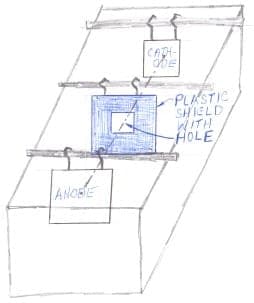
Where that isn't practical, shields are usually the best answer. These are non-conductive plastic plates that are placed between the anode and the cathode so that the current cannot take a direct path through them, but must go around the shields, or only through limited holes in them. In your case, conceptually you might have a shield with a rectangular hole in it that is smaller than the cathode, so that the current must travel a long way to get to the edges and corners. (In my sketch the distance from the shield to the cathode is exaggerated so things aren't drawn on top of each other and thus invisible; in reality the shield would probably be only a couple of inches from the cathode and even closer if the cathode is very small).
The design of shields can be an art or a science. Experienced electroformers will have a good feel for how to make a geometrically appropriate shield, and how to tweak it to improve it, and software is also available for the purpose. Good luck.
Regards,
Ted Mooney, P.E.
Striving to live Aloha
finishing.com - Pine Beach, New Jersey
Need quick confidential answers? $25
Need project assistance? $100/hr.
Q. Thank you for your response Mr Mooney. I however, tried the shielding solution before. Unfortunately, it did not give any results for some reason. I will keep experimenting with it. I would like to ask you another solution named "Pulse plating". I am planning a forward/reverse dc current application. In order to foresee if this works or not, I want to measure the current distribution on the metal plate. How do you think that would be possible ? Also, would you guess, the current distribution on the surface of the plate changes linearly with the amount of current amperes applied?
Also in this pulse plating, I have concerns about the brightness of the end product. What do you think of these issues ?
Best regards,
Ozum
- London England
February 9, 2014
A. Hi again. Shields have to work, Ozum. Plating will not deposit where there is no current flow, will deposit lightly where is is little current flow, and will deposit heavily where there is high current flow. Picture a shield very close to the object you are plating, and with only a pinhole in the center. All of the plating would of necessity be right by the pinhole; there would be no plating at all at the corners. I suspect your shields are too far from the cathode and/or the holes are too big to be effectual.
Pulse plating can be of some value by chasing ions back through the boundary layer during the reverse current portion of the cycle, but it is yet another difficult variable to tame in a process that you are already having some trouble with.
Nickel plating is quite efficient, about 95%+, across the plating range -- so your plating thickness map is already a quite accurate current density map; you don't need to develop and alternate way to check it. Good luck.
Regards,
Ted Mooney, P.E.
Striving to live Aloha
finishing.com - Pine Beach, New Jersey
Need quick confidential answers? $25
Need project assistance? $100/hr.
February 2014
Q. Hello again Mr. Mooney,
Thank you for your reply. I would like to clarify my application. I am electroforming small letters, 1 cms in height and about 7mm in width. Considering the complex shapes letters have, it was not easy to obtain the shield. However I managed to make one. Basically when you try to fit the shield to the letter, the whole in the shield which is shaped as that letter I want to form, come across to the letter in a way that is completely contained by the letter I want to form. You can visualize it as an "V" letter in a bigger "V". Hence, I aimed to lower the nickel growth in the edges. But there was not even an improvement.
My suspicion also lies on another fact that the photo mask I have used to create the letter on the mandrel, was 2500 dpi. Is it possible that the edges have so many micro corners caused by the lower pixel resolution mask, that these extra corners unseen by the human eye, causes excessive current density ?
I am really puzzled as my research shows so very little people ever complain about the overgrowth in the edges. I am quite unsure what the problem is. I could provide images if you think that would help, but I really can't sort out how to do it as you did with your sketch in your previous answer.
Thanks again for your attention.
- London England
February 10, 2014
February 2014
Hi. We are leaving my area of experience. Hopefully another reader will be able to comment on your situation. Good luck.
Regards,
Ted Mooney, P.E.
Striving to live Aloha
finishing.com - Pine Beach, New Jersey
Need quick confidential answers? $25
Need project assistance? $100/hr.
A. Hello Ozum,
Let's get down to basics. What current density are you applying? As you may know from your research, a higher current density will favor the high current density areas. When you lower the current density, you will achieve a more uniform thickness across the part to be plated. What Ted had recommended with shielding and anode to cathode spacing makes perfect sense. What is the anode to cathode spacing? What is the anode to cathode ratio? Is there cathode bar movement? How about solution agitation? If you will answer these questions we can better get an idea of how to help you. Please advise.
process engineer - Malone, New York
February 11, 2014
Sorry! Finishing.com is temporarily Read-Only.
Ted Mooney is retiring but I have several offers to take it over.
We're working hard to make sure we find it the best new home.