-----
Applying Metallization to Barium Titanate Ceramics
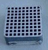
Q. The device referred to is a grid-shaped ceramic bodymade from barium titanate. It is about 24 x 24 mm across and has a depth of about 10 mm. It has 81 square-shaped channels passing through it, at a right angle to the larger surfaces. An adhering metallization is applied to the inside walls of these passages so that they can be used as electrode surfaces, making the walls themselves the actual resistor. The cells are connected to positive and negative in an alternating pattern like this:
 _____________
|+ - + - + -|
|- + - + - +|
|+ - + - + -|
|- + - + - +|
|+ - + - + -|
-------------
To interconnect cells of positive or negative polarity, thin conductive strips must run diagonally between them. The problem is: How can an adherent metallization be applied in a way that there are non-conductive zones between the + and - diagonal rows of cells; and is it possible to apply metallization to the inside of the cell walls in a uniform thickness of about 15µm? What material is best suited for that?

The parts onto which metallizing is to be applied look more or less like this. The conductive stripes run from the upper left to the lower right corner interconnecting the openings along the way, and the inside of these openings is to be metallized. How can this be done in one step? Somewhat akin to the etching of PCB's with photoresist? And what solutions are recommended as not to harm the ceramic substrate (doped barium titanate)?
Thanks a lot
- Munich, Germany
2000
A. Sorry I don't understand your explanation, but why can't you metallize the non-conductors the same way that we make printed wiring boards, stannous chloride sensitizing, palladium chloride activation, followed by electroless copper or electroless nickel?

Tom Pullizzi
Falls Township, Pennsylvania
2000
Q, A, or Comment on THIS thread -or- Start a NEW Thread