-----
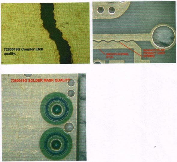
Jagged edge on plating
We have received some prototypes of PCB from a supplier with jagged edge on some areas.
The plater claims that it is due to the thickness of Gold (>50µinch) and Ni (>200µinch) that is needed on the boards that produces such observation. This is the same supplier who said that we cannot have a 1:1 ratio of gold over nickel ( I have posted this question before in the forum).
I think this cannot be the reason, my thought is that the jagged plating can only 'grow' out of something that is already jagged and that is from the copper and in turn that would probably be from the mask.
Comments please because I need to resolve the criteria although it may not affect the performance of my circuit.
 Sam Tan
engineer - Singapore
2004
Without knowing more about the precise PCB fabrication process, I would suggest the fault lies in either the photomask or in some aspect of the photoresist.

Trevor Crichton
R&D practical scientist
Chesham, Bucks, UK
2004
You are right, we got the artwork from the supplier and indeed the edges are jagged. Thank you very much.
Sam Tan- Singapore
2004
Q, A, or Comment on THIS thread -or- Start a NEW Thread